Let’s go into more detail on how the BJT (bipolar junction transistor) works.
The last article on transistors (An Introduction to Transistors) started with a little history on the devices and what was in use before them. Then, it glossed over the two main types you’ll work with: BJTs and MOSFETs. Finally, the two modes of transistor operation were briefly discussed.
This time, we’re going to take a deeper dive into BJTs specifically. This article will go into a bit more detail on how the BJT or bipolar junction transistor works and some basics on using them in your creations.
How BJTs Work
BJT Basics Recap
Let’s start with a quick recap on the basics of how a BJT works.
I won’t regurgitate every single word about BJTs from the last article but for the sake of convenience I’ll present a quick review on the fundamentals.
However, if you’re just learning about transistors I suggest you first read How Diodes Work – An Introduction because it talks about basic semiconductor principles and then read An Introduction to Transistors.
Recall that there are two main types of BJTs and that the BJT is a three terminal device, as we can see in figure 1. The three terminals are the base, collector, and emitter.

Figure 1: the two main types of bipolar junction transistors are NPN and PNP.
An NPN BJT sandwiches P-type semiconductor material between two layers of N-type semiconductor material. Conversely, a PNP BJT sandwiches N-type material between two layers of P-type material.

Figure 2: conceptual structure of a PNP and an NPN BJT.
Finally, a BJT can find use as either a switch or an amplifier.
How a BJT Works: A Closer Look at Structure
The name bipolar junction transistor may make one think that the device has an unfortunate mental health issue. Of course, this is not the case.
The term bipolar means the device is made from semiconductor material in which conduction relies on both positive and negative charge carriers. These “charge carriers” are holes and electrons, respectively.
Figure 2 suggests that the three silicon regions of a BJT are segments of a bar which stack on top of each other (if you rotate the pic 90 degrees). While some of the first transistors from the late 1940s and early 1950s were made this way, modern transistors are not.
Figure 3 depicts the structure of a modern BJT.
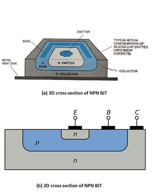
Figure 3: structure of a modern BJT.
As we can see, the layers do not stack on top of one another. Instead, semiconductor manufacturers use a diffusion process which melts the base into the collector region and then melts the emitter region into the base region (for an NPN BJT). Thousands of transistors are diffused on a silicon wafer from which induvial transistors are then cut before being sealed in plastic or metal.
One last thing to note about BJT structure is that the base region is lightly doped and very thin compared to the heavily doped emitter and moderately doped collector regions. The reason for this will become apparent shortly.
How a BJT Works: Low Level Operation
It’s time to get into some detail about how BJTs work. First, we’ll start with some basic low-level operation before going into more practical high-level operation.
To illustrate how a BJT works, let’s take a look at what happens inside an NPN transistor. It will be helpful to think of the base-emitter (BE) and base-collector (BC) junctions as diodes, like figure 4 depicts.
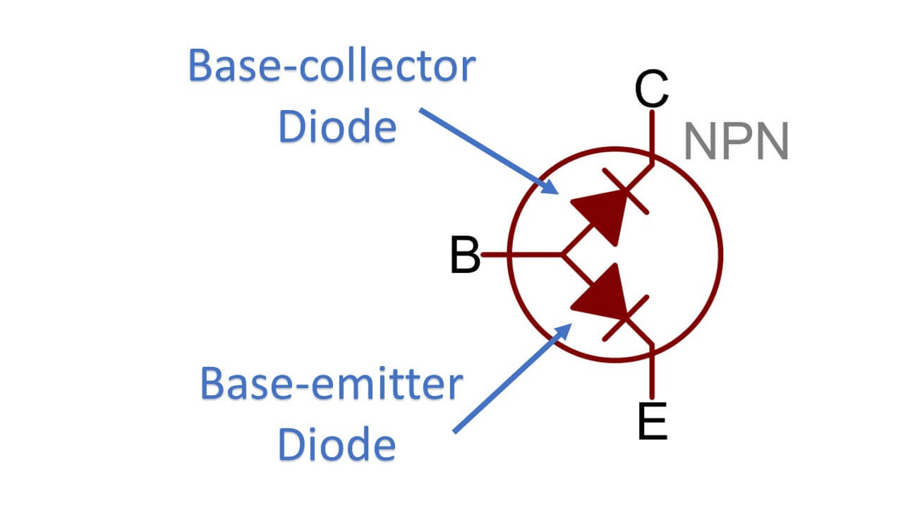
Figure 4: it’s helpful to visualize the junctions in a BJT as diodes. If this were a PNP BJT each diode would be turned 180 degrees.
First, let’s talk about what happens when the transistor is off.
Remember that a typical silicon diode needs about 0.7 V to turn on and conduct. So, with less than 0.7 V on the base the transistor is off because the low voltage does not forward bias the BE diode. If we were to apply a negative voltage to the NPN BJT in figure 4 the situation worsens; the p-n junction between the base and emitter widens.
Applying a voltage of at least 0.7 V forward biases the BE diode and the transistor begins to turn on. As the voltage increases the depletion zone narrows and electrons head toward the positive base. Remember that the emitter is heavily doped and contains an excess of free electrons.
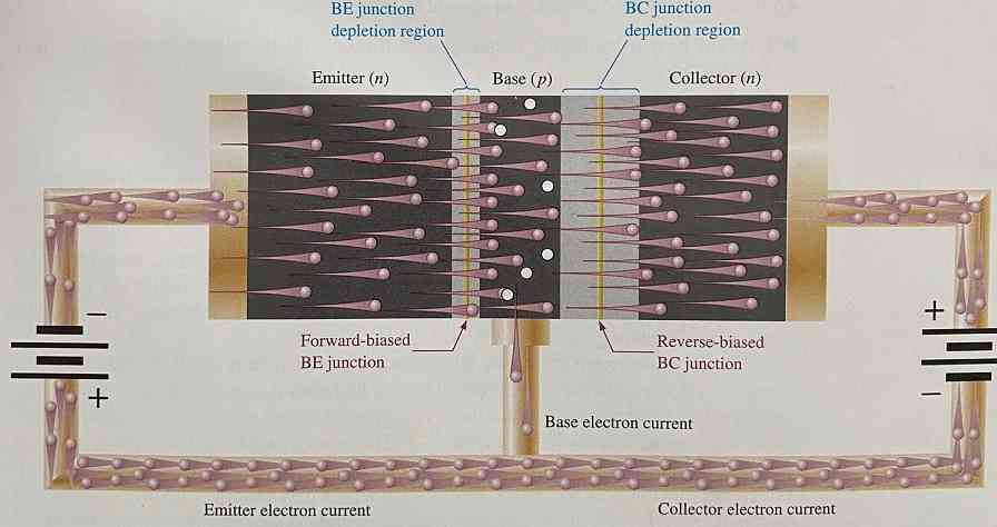
Some of them will exit through the base but because it’s so thin with a light doping most of them (like more than 97%) that leave the emitter will get close enough to the collector side that they begin to jump into the collector. Increasing the base voltage increases this effect. During this time the BC diode is actually reversed biased, but the electric field set up by the collector supply voltage pulls the electrons through. It is this that makes the BJT act as a variable resistor; the wider the depletion region of the BC diode, the more resistance the device offers.
In fact, any properly biased NPN BJT for use in amplification will have a forward biased BE junction (emitter diode on) and a reversed biased BC junction (collector diode off).
Ever dreamed of being Iron Man, having the ability to build anything, anytime? Try Academy for Arduino!

Figure 5 below offers a graphical view of this process.

Figure 5: how a BJT works on a low-level. This is how electrons move through an NPN BJT. Note the picture uses electron flow rather than conventional current flow. The small white circles in the base are holes. Some electrons will combine with the holes in the base.
Notice that since the base is a p-type material it contains holes.
Here’s another way to think of NPN BJT operation: for every hole that is filled in the base by an electron, a small negative charge is trapped in the base terminal. The only way to get rid of the charge is to draw electrons from the base. So, to maintain collector current all electrons that fall into holes need to be drained. This is why the base current controls the collector current.
How a BJT Works: The Practical Side or High Level Operation
Now that we know something about low-level BJT operation, let’s talk about the more practical, higher-level operation of the device.
A BJT uses a small current at its base to control a much larger collector current.
Before we go any further, it may be useful to define some important terms concerning the operation of a bipolar junction transistor.
Saturation refers to a region of operation where maximum collector current flows and the BJT acts like a closed switch from collector to emitter. In this mode the BC junction forward biases and maximum current flows. The collector current cannot increase any more, even with an increase in base current.
Cutoff refers to a region of operation where the BJT acts like an open switch, though a very small leakage current (which we can usually neglect) still flows.
Finally, the active mode or active region describes operation in which the BE junction is forward biased, and the BC junction is revered biased. In this mode, the BJT is equivalent to a variable resistor between the emitter and collector. If we want to use a bipolar junction transistor for amplification, we need to operate it in this mode or region.
Figure 6 graphically depicts these modes of operation with a family of collector characteristic curves. Here, several values of IB are used to plot IC vs VCE. The cutoff region lies along the horizontal axis. The saturation region is the area to the left of the near-vertical line. The straight, horizontal lines represent the active region. Put another way, these curves describe the effects the base current and emitter-to-collector voltage have on the emitter / collector currents.
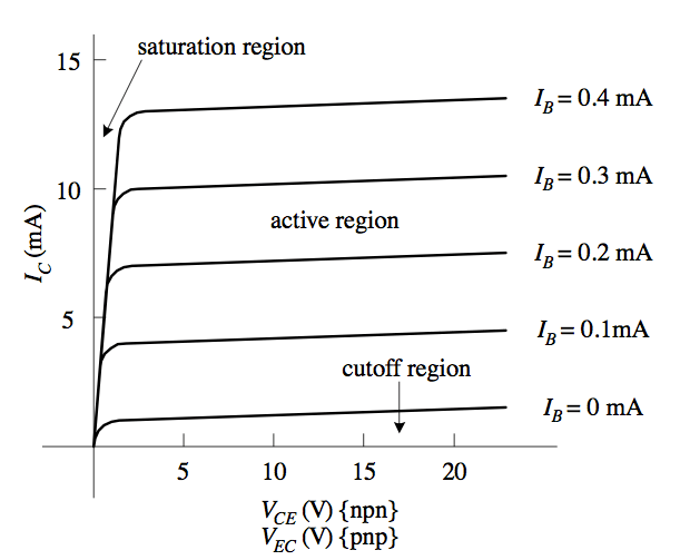
Figure 6: BJT collector characteristic curves show how a BJT works for the 3 modes of operation.
Equation 1 gives the total current flowing in the emitter of a BJT. Since the base current IB is very small compared to the collector current IC, it is usually neglected and equation 2 suffices for most applications.
IE = IC + IB (eq. 1)
IE ≈ IC (eq. 2)
We already know that a small base current causes a larger collector current to flow. Bipolar junction transistors relate the current flowing into the base and the collector current through a constant beta (ẞ). Beta is also sometimes referred to as hFE. Every single BJT has its own unique beta value ranging from 20 to 500. This is the transistor’s current gain. Equation 3 gives the formula for current gain as it relates to total beta and total collector current.
IC = ẞIB (eq. 3)
There are few important things to note about equation 3.
First, the BJT needs to be in the active region of operation for it to apply. For this to be the case there are two rules that we need to heed.
Rule 1: The voltage at the collector must be at least a few tenths of a volt higher than the voltage at the emitter. This applies to NPN BJTs. For PNP BJTs, the emitter voltage must exceed the collector voltage by a similar amount. If this condition isn’t met, no current flows through the device regardless of the base voltage.
Rule 2: There is a voltage drop of about 0.7 V from base to emitter in an NPN BJT and a rise of 0.7 V from base to emitter for a PNP device. Using an NPN transistor as an example, this means that the base voltage must be at least 0.7 V higher than the emitter voltage to overcome the diode drop. If this isn’t the case, the transistor will not turn on. Equation 4 expresses this rule mathematically.
VBE = VB – VE = 0.7 V (or -0.7 V for a PNP device) (eq. 4)
Another less-often used constant pertaining to BJTs is the device’s alpha (α). Alpha describes the ratio of the DC collector current to the DC emitter current.
α = IC/IE (eq. 5)
Also:
α = ẞ / (ẞ + 1) (eq. 6)
Typical values of alpha range from 0.95 to 0.99 or more but it is always less than 1.
Before we go any further, a simple example will help us analyze BJT circuits at DC.
Ex 1:
Refer to the figure below. Assume a beta of 150 and that RC = 100 Ω and RB = 10k Ω. Find IB, IC, IE, VBE, and VCB. VBB = 5 V and VCC = 10 V.

Solution:
We know that VBE is about 0.7 V. We’ll use that info to get IB as follows:
IB = (VBB – VBE) / 10k = (5 – 0.7) / 10k = 430 µA
The equation above may be hard to understand for those new to electronics, but it’s just a basic application of Ohm’s Law. Since VBB is 5 V and VBE is 0.7 V, 4.3 V must drop across the base resistor. Once we know this, finding the base current is a cinch. If this is still confusing reading Simple Circuit Analysis Techniques You Should Know may help.
Onto IC…
IC = ẞIB = (150)(430 µA) = 64.5 mA
Let’s grab IE next…
For most purposes it may be okeydokey to approximate and say that IE = IC = 64.5 mA.
If we want to be exact, we can say IE = IB + IC = 430 µA + 64.5 mA = 64.9 mA. Notice there isn’t much of a difference.
Now for VCE:
Applying Ohm’s Law, we get VCE = VCC – ICRC = 10 V – (64.5 mA)(100) = 10 V – 6.45 V = 3.55 V
Finally, let’s get VCB:
VCB = VCE – VBE = 3.55 V – 0.7 V = 2.85 V
Remember that the relation IC = ẞIB is only valid for transistors in the active region and does not work for transistors in saturation.
Let’s do another slightly different example to illustrate how a BJT works.
Ex 2:
Take a gander at the circuit below. Beta is 100. Determine all node voltages and branch currents.

The base it at 4 V and the emitter is at ground, so it’s safe to assume that the BE junction is forward biased.
VE = 4 – VBE = 4 – 0.7 = 3.3 V
Now let’s get IE:
IE = (VE – 0) / RE = 3.3 / 3.3k = 1 mA
We don’t know the base current yet, but we can rearrange equation 5 by multiplying both sides by IE:
IC = αIE
Next let’s use equation 6 to find alpha:
α = ẞ / (ẞ + 1) = 100/101 = 0.99
Now we can get IC:
IC = (0.99)(1 mA) = 0.99 mA
Using Ohm’s Law, we can grab the collector voltage:
VC = 10 – ICRC = 10 – ((0.99 mA)(4.7k)) = 5.3 V
Finally, we need the base current:
IB = IE / (ẞ + 1) = 1 mA / 101 = 0.01 mA
BJTs in Saturation: The Transistor as a Switch
Unless you’re into designing amplifiers and analog circuits you’ll probably be using the BJT as a switch most of the time.
Some may ask why bother using a transistor as a switch when we can just use a mechanical switch. There are a few good reasons for this. First, transistors can switch on and off extremely fast, typically a fraction of a micro-second or less. Second, they can be driven from other circuits (such as a microcontroller) whereas a mechanical switch cannot. Mechanical switches wear out and the contacts bounce while transistors do not. And there are other reasons. If you’re still not convinced transistors make good switches, you’ll just have to take my word for it.
When using a bipolar junction transistor as switch, you’ll operate it in cutoff and saturation modes.
Cutoff mode is self-explanatory – the device is off and is not conducting any current (except for a negligible leakage current).
In cutoff, equation 7 holds true.
VCE = VCC (eq. 7)
When the BE junction is forward biased and there is enough base current to produce a maximum collector current the transistor is saturated. Equation 8 gives the formula for collector current when the device saturates.
IC(sat) = (VCC – VCE(sat)) / RC (eq. 8)
Normally VCE(sat) is very small compared to VCC (the BJT is acting like a closed switch and there is ideally 0 V across a closed switch because it’s a short) and we can neglect it. The minimum base current the BJT needs for saturation is:
IB(min) = IC(sat) / ẞ (eq. 9)
Note that IB should be significantly greater than IB(min) to be sure the BJT stays well into saturation.
Finally, some inquisitive readers may be asking if there is a formula for VCE(sat). Indeed, there is, but as we’ve mentioned this quantity can usually be neglected and the formula involves some complexity that’s beyond the scope of this writing.
Let’s do a quick, practical example of how a BJT works in saturation as a switch.
Ex 3:
The LED in the figure below needs 30 mA to emit an aesthetically pleasing level of light. So, the collector current should be about 30 mA. Determine the amplitude of the DC signal the transistor needs to saturate and light the LED. Use double the minimum base current as a safety margin because ruining the mood lighting (by having the LED turn off) would make her want to leave. Vcc = 9 V, VCE(sat) = 0.3 V, Rc = 270 Ω, RB = 3.3 kΩ and ẞ = 50.
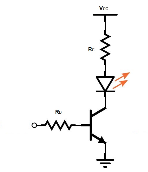
Let’s get Ic:
Ic = (Vcc – VCE(sat)) / Rc = (9 V – 0.3 V) / 270 Ω = 32.2 mA
IB(min) = IC(sat) / ẞ = 32.2 mA / 50 = 644 µA
Next let’s double the minimum to ensure saturation so our date sticks around. This gives us about 1.29 mA.
Now:
IB = VRB / RB = (Vin – VBE)) / RB = (Vin – 0.7 V) / 3.3 kΩ
Solving for Vin
Vin – 0.7 V = 2IB(min) * RB = 1.29 mA * 3.3 kΩ
Vin = (1.29 mA)(3.3 kΩ) + 0.7 V = 4.96 V
Some Final Thoughts on BJTs
Let’s wrap this up with a few final tips and thoughts on BJTs.
We know that the beta of any random BJT varies widely. Because beta is somewhat unpredictable, you should avoid designing and building circuits that depend specifically on beta values to work correctly. In other words, a circuit that depends on a particular value of beta is a bad circuit.
Also, all transistors have a maximum collector current rating as well maximum collector to base, emitter to base, and collector to emitter breakdown voltages. You also need to be aware of the maximum power dissipation rating. Ignoring these specs can kill your BJT.
Bipolar junction transistors come in a variety of packaging types. Some come in plastic, others in metal can-like packages. Look at the package to see if it has a pinout diagram on it. If it doesn’t, a good cross-reference (like NTE) of the Internet can help. If all else fails, you may have to use the transistor tester in your meter or “Ohm it out” if it doesn’t have one.
Testing a BJT
Speaking of multimeters, yours may come in handy for testing transistors you suspect may be bad.
Remember how a BJT works — its like two diodes.
A good diode shows high resistance with reverse bias and a low resistance with forward bias. An open diode will have a high resistance both ways. A shorted diode will have low resistance both ways. Many modern DMMs sport a diode and/or transistor test function to make this easier.
That wraps up our intro to BJTs. Next time we talk about them we’ll go over some basic biasing techniques.
Meanwhile, leave a comment and tell me about your latest endeavor using discrete BJTs. What are you driving? An LED? Speaker? Motor? Something else?
Share it!
Ever dreamed of being Iron Man, having the ability to build anything, anytime? Try Academy for Arduino!

Electronics Tips & Tutorials Sent Directly to Your Inbox

Submit your email & you'll get:
- Exclusive content that I don't put on the blog
- The checklist 10 mistakes all electronics enthusiasts make (& how to avoid them)
- And more!
Thank you very much.
You’re very welcome!
This short course is exactly what I needed.
Correct me if I’m wrong, but in Example #3, it appears that the calculations were made based as if the led was missing from the circuit.
Don’t think so, it says the LED needs 30 mA in the problem. Did you get a different answer?